Hi Steve, Hi all,
Steve: Thanks! I did confuse brass and bronze in what I wrote! I appreciate you taking the time to make that right!
As for diodes switching on and off or open and closed, I am sorry I used that language in that post. It apparently wasn't at all helpful and, from the reactions I've gotten, has been quite the distraction! Having said that, I actually think it was correct (be it totally unhelpful). So, for anyone curious, I am going to explain it. If I'm wrong -- I'm all ears. Pretty please do let me know. I don't deal with things at this level of detail very often. My model could have been corrupted at some point and I just don't realize it. I'd much rather learn than continue to be wrong about it.
My model of a diode includes a P(anode) region and an N(cathode) region. In the N region there are some covalent bonds among the materials in the lattice that leave electrons unbound and in the P region, there are some covalent bonds in the lattice that are missing electrons. These are the results of secondary materials that off balance things being "duped" into the lattice. The imbalance that results from the free electrons (extra electrons) and free holes (missing electrons) is balanced out by much weaker ionic bonds (opposites attracting versus sharing of electrons between atoms). The N side and the P side can each have N and P imbalances that go both ways, but the N side has more favoring free electrons and the P side has more favoring missing electrons (holes).
Without some more magic, this wouldn't matter much because, even if by a mixture of bond types, the N side and the P side are each neutral in charge. There is no electrical or magnetic force acting between them. But, by careful manufacturing what can happen is that some of the free electrons, being weakly connected anyway, are able to be pulled over the border by "opposites attracting" and fill in the holes on the other side. This starts to generate a region where the two come together that is out of balance. It is relative positive where the electrons left and relatively negative where the holes got filled. There is only so much force pulling, so eventually enough electrons cross over that they manage to repel other electrons from coming over (opposites attract, but sames repel). And, given the distances, this happens pretty quickly, making for a relatively thin "cross over" zone.
These weakly connected electrons and available holes are known as "charge carriers" because they allow current to flow. When motivated by potential energy (voltage), electrons can jump, leaving a hole where they left and filling one where they go to. This is why electron flow and hole flow are said to be opposites. As an electron moves one way, a hole seems to move the other.
But, back to the diode. With this movement, something interesting has happened. We've ended up with this thin area between the P region and the N region that is depleted of available charge carriers. For this reason, it is sometimes called the "depletion zone". It also has a local charge to it, owing to the imbalance. For this reason it is sometimes called the "space charged zone" There is actually "potential difference" (voltage) across it because of that imbalance. But, at least at rest, there is no current flow, because everything that could flow did.
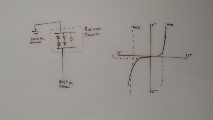
This local potential difference is sometimes called the built-in voltage of the diode and symbolized Vbi. It is somehow related to the voltage drop of the diode that we all know and love, e.g. about 0.7V for silicon diodes. I'm going to wave my hands and rhetorically suggest asking William Shockley. I don't know the relationship between the two, and don't think I ever did. The only thing I remember is that the threshold voltage drop varies with the current flow and temperature and some other parameters, but so very little that it doesn't matter within the application space of the device.
Regardless, back to that threshold voltage. What happens if we apply a "forward voltage" to a diode, i.e. generate an imbalance with electron donors on the N side and holes on the plus side? For low enough voltages, absolutely nothing we can see from the outside. The potential differences asserts a fore that overcomes some of the "opposites attracting" thing and the depletion zone gets smaller. But, current still can't flow at all -- because the depletion zone still exists and it is an insulator. But, at a certain point, we apply enough of a voltage to overcome the opposites attracting thing, the depletion zone collapses....and now we have an area with free electrons directly up against one with free holes and a potential difference across them. Like magic, we've got a bunch of electrons being driven to hope from hole to hole to hole. We've got current flow!
Even after current starts to flow, the voltage drop doesn't go away, because it is still pushing against the imbalance that created the depletion zone at the PN junction. But, as many electrons go in one one side as come out the other. And, the opposite is true: As many holes appear on one side as disappear from the other. Once a diode switches on, it is on, it does not limit current flow.
This is why I referred to a forward biased diode at or above Vth as being like a switch that is "closed" or "on" and otherwise being like a switch that is "open" or "off". Like a switch in the "On" state, a diode above Vth allows unrestricted current flow, and otherwise, like a switch in the "off" state, allows none.
Does it work exactly like this? Well, nothing ever does. But, the voltage-current curve is extremely steep on the forward voltage side of the graph as to be a really darn good approximation of a vertical line. For all intents and purposes in normal applications, I think it is on and off.
Just for completeness, what happens if one reverse biases a diode? Well, for a while, nothing at all. There are a bunch of free holes one one side that already has a bunch of free holes. And, there are a bunch of free electrons on a side that has a bunch of free electrons. The polarity of the diode prevents current flow. And, in fact, just as a forward bias acts to shrink the depletion zone -- a reverse bias acts to grow it. And, this is how, in many applications, diodes are used as "gate valves", allowing current to flow in one directions, but not another. One classic examples include the first step of converting AC power into DC, i.e. rectifying each phase of it.
But, at a certain point the potential difference is sufficient for current flow to happen in reverse. Something called the "Zener effect" kicks in and allows electrons to jump across the boundary. And, beyond that, something called the "Avalanche effect" kicks in, which is pretty unfortunate. Bound electrons get energized and break free and knock others free. This generates a lot of current and heat, which can let the smoke out.
Some diodes are designed to survive being reverse biased enough to allow current flow, at least up to some maximum voltage or power rating. These diodes are known as "Switching diodes" because different diodes can be designed with different break down voltages to "switch" on and off at different voltages depending upon how the depletion zone is engineered, etc. They can work at certain voltages by favoring Zener switching to avalanching. But, most are, I think, just designed to operate within part of the avalanche curve by dissipating the heat well.
Regardless, back to our friend the galvanic isolator. I've attached a picture of what a basic galvanic isolator looks like in my mind. It includes two pairs of two diodes each. Each pair has two diodes in series and oriented the same way. The two pairs are wired in parallel, but in opposite orientations. The effect of this is that voltage in excess of ~1.4V (2* ~0.7V) in either direction will "switch on" the diode pair oriented in that direction, "closing" the diode just like "closing" a switch, allowing current to flow. But, voltages less than ~1.4V in either direction won't be sufficient to "Switch on" the diode pair, leaving the diodes "switched off" and leaving the ground path "open", just like an "open switch".
It also includes a capacitor, wired in parallel, because capacitors will pass AC but not DC (DC saturates them, so somewhat like a fully battery, they don't let more juice flow, whereas AC keeps reversing, so it just time shifts the current and voltage curves, but doesn't prevent current flow). So, the capacitor won't let DC stray current pass through, but can do two things. The first is provide a way to let AC current that leaks to ground on the boat, such as from surge supressors, leave the boat via the ground-- without saturating the diodes, switching them "on" and thereby letting DC stray current through with the AC leak current. The second is to provide a back-up path for AC to leave the boat if a diode fails and remains as an "open switch" even when it should "switch on" or "closed" to let fault AC out.
I've never tried to build my own galvanic isolator. I don't put science experiments on my boat. So, I've never thought about (a) if there should normally be enough leakage to make it worth the capacitor for that purpose (or if such leakage should simply be fixed). Nor have I thought about whether or not the diodes are likely enough to fail to need a capacitor as a back-up path. Nor have I thought about whether or not I could select a capacitor such that it could serve both purposes, or if I would need to pick one or the other. On my own boat, I installed an ELCI, so, although I've never measured, any AC leakage current on my boat must be somewhat low.
So, back to my question...my belief is that, with a voltage of less than ~1.4V the diodes are "switched off/open" and no current is flowing along the path, despite the potential and current course. And that voltages above ~1.4V "Switch the diode on/closed", allowing current to flow along the path. And that at least one purpose of a parallel capacitor is to prevent leaking a relatively small amount of leaking AC current from "Switching on" a diode pair (half the time) allowing DC current through, even thought eh DC current is below the ~1.4V threshhold.
Basically, I really do think the diodes operate as voltage-controlled switches.
What am I missing here?
Thanks!
-Greg
") .
.